- 您现在的位置:买卖IC网 > Sheet目录319 > CS5463-IS (Cirrus Logic Inc)IC PWR/ENERGY METER 2CH 24-SSOP
�� �
�
�CS5463�
�SWITCHING� CHARACTERISTICS� (Continued)�
�Parameter�
�Symbol�
�Min�
�Typ�
�Max�
�Unit�
�E1,� E2,� and� E3� Timing� (Note� 19� and� 20)�
�Period�
�Pulse� Width�
�Rising� Edge� to� Falling� Edge�
�E2� Setup� to� E1� and/or� E3� Falling� Edge�
�E1� Falling� Edge� to� E3� Falling� Edge�
�t� period�
�t� pw�
�t� 3�
�t� 4�
�t� 5�
�250�
�244�
�6�
�1.5�
�248�
�-�
�-�
�-�
�-�
�-�
�-�
�-�
�-�
�-�
�-�
�?� s�
�?� s�
�?� s�
�?� s�
�?� s�
�Notes:� 19.� Pulse� output� timing� is� specified� at� MCLK� =� 4.096� MHz,� E2MODE� =� 0,� and� E3MODE[1:0]� =� 0.� Refer� to�
�Section� 5.5� Energy� Pulse� Output� on� page� 17� for� more� information� on� pulse� output� pins.�
�20.� Timing� is� proportional� to� the� frequency� of� MCLK.�
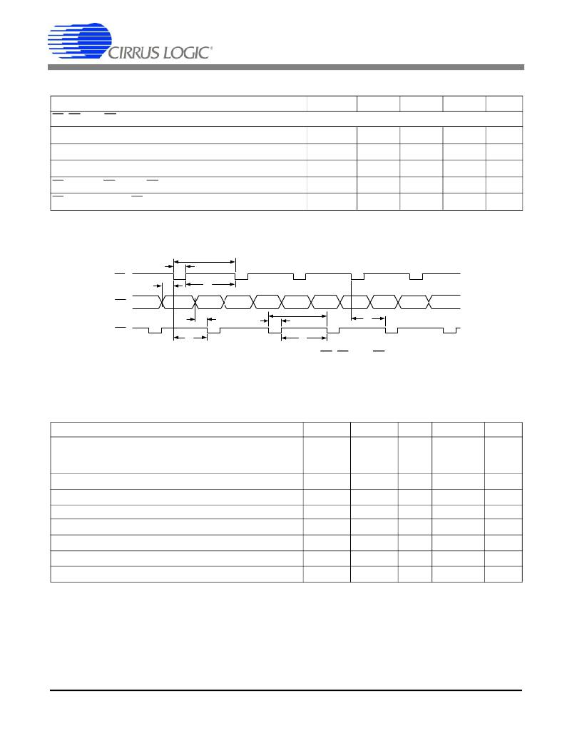
�t� pw�
�t� period�
�E1�
�E2�
�t� 4�
�t� 3�
�E3�
�t� 4�
�t� 5�
�t� pw�
�t� period�
�t� 3�
�t� 5�
�Figure� 2.� Timing� Diagram� for� E1,� E2,� and� E3�
�ABSOLUTE� MAXIMUM� RATINGS�
�WARNING:� Operation� at� or� beyond� these� limits� may� result� in� permanent� damage� to� the� device.�
�Normal� operation� is� not� guaranteed� at� these� extremes� .�
�Parameter�
�Symbol�
�Min�
�Typ�
�Max�
�Unit�
�DC� Power� Supplies�
�(Notes� 21� and� 22)�
�Positive� Digital�
�Positive� Analog�
�VD+�
�VA+�
�-0.3�
�-0.3�
�-�
�-�
�+6.0�
�+6.0�
�V�
�V�
�Input� Current,� Any� Pin� Except� Supplies�
�(Notes� 23,� 24,� 25)�
�I� IN�
�-�
�-�
�±10�
�mA�
�Output� Current,� Any� Pin� Except� VREFOUT�
�I� OUT�
�-�
�-�
�100�
�mA�
�Power� Dissipation�
�Analog� Input� Voltage�
�Digital� Input� Voltage�
�Ambient� Operating� Temperature�
�Storage� Temperature�
�(Note� 26)�
�All� Analog� Pins�
�All� Digital� Pins�
�P� D�
�V� INA�
�V� IND�
�T� A�
�T� stg�
�-�
�-� 0.3�
�-0.3�
�-40�
�-65�
�-�
�-�
�-�
�-�
�-�
�500�
�(VA+)� +� 0.3�
�(VD+)� +� 0.3�
�85�
�150�
�mW�
�V�
�V�
�°C�
�°C�
�Notes:� 21.� VA+� and� AGND� must� satisfy� [(VA+)� -� (AGND)]� ?� +� 6.0� V.�
�22.� VD+� and� AGND� must� satisfy� [(VD+)� -� (AGND)]� ?� +� 6.0� V.�
�23.� Applies� to� all� pins� including� continuous� over-voltage� conditions� at� the� analog� input� pins.�
�24.� Transient� current� of� up� to� 100� mA� will� not� cause� SCR� latch-up.�
�25.� Maximum� DC� input� current� for� a� power� supply� pin� is� ±50� mA.�
�26.� Total� power� dissipation,� including� all� input� currents� and� output� currents.�
�DS678F3�
�13�
�发布紧急采购,3分钟左右您将得到回复。
相关PDF资料
CS5464-IS
IC PWR/ENERGY METER 3CH 28-SSOP
CS5466-ISZR
IC ENERGY METERING 1PHASE 24SSOP
CS5466-IS
IC ENERGY METERING 1PHASE 24SSOP
CS8312YN8
IC PREDRIVER IGBT IGNITION 8DIP
CX1006
SOCKET ADAPTER 40TSOP SUPERPRO5K
CYCLONEMAX
CYCLONE MAX FLASH PROGRAM
D-1723-WH
DRAWER SLIDING 16.56X6.31X19.18"
D072-0103
DEV KIT 7 NIMBLE SBC/FUSION7/BB
相关代理商/技术参数
CS5463-ISZ
功能描述:电流和电力监控器、调节器 Single Phase Power/Energy IC RoHS:否 制造商:STMicroelectronics 产品:Current Regulators 电源电压-最大:48 V 电源电压-最小:5.5 V 工作温度范围:- 40 C to + 150 C 安装风格:SMD/SMT 封装 / 箱体:HPSO-8 封装:Reel
CS5463-ISZ/D
制造商:Cirrus Logic 功能描述:
CS5463-ISZR
功能描述:电流和电力监控器、调节器 IC Single Phase PWR/Energy RoHS:否 制造商:STMicroelectronics 产品:Current Regulators 电源电压-最大:48 V 电源电压-最小:5.5 V 工作温度范围:- 40 C to + 150 C 安装风格:SMD/SMT 封装 / 箱体:HPSO-8 封装:Reel
CS5463-ISZR/E2
制造商:Cirrus Logic 功能描述:
CS5464
制造商:CIRRUS 制造商全称:Cirrus Logic 功能描述:Three-channel, Single-phase Power/Energy IC
CS5464_07
制造商:CIRRUS 制造商全称:Cirrus Logic 功能描述:Three-channel, Single-phase Power/Energy IC
CS5464_11
制造商:CIRRUS 制造商全称:Cirrus Logic 功能描述:Three-channel, Single-phase Power/Energy IC
CS5464-IS
功能描述:电流和电力监控器、调节器 3-Ch Single Phase Power/Energy IC RoHS:否 制造商:STMicroelectronics 产品:Current Regulators 电源电压-最大:48 V 电源电压-最小:5.5 V 工作温度范围:- 40 C to + 150 C 安装风格:SMD/SMT 封装 / 箱体:HPSO-8 封装:Reel